

What you'll learn
- Why light microscopes cannot see atoms, and how wave-particle duality offers a solution.
- How to estimate the anode voltage required to give electrons an atomic-scale de Broglie wavelength.
- The operating principles of the Transmission Electron Microscope (TEM).
- How the Scanning Tunnelling Microscope (STM) uses quantum tunnelling and piezoelectric crystals to map surfaces.
Overcoming the limits of light
In a traditional optical microscope, resolving fine details is limited by diffraction. When light waves pass through a gap or around an object similar in size to their wavelength, they spread out. Because visible light has a wavelength between roughly 400 nm400 \text{ nm}400 nm and 700 nm700 \text{ nm}700 nm, any object smaller than this (like a virus or an individual atom) simply diffracts the light, blurring into an unresolvable fuzz.
To see atoms—which are roughly 0.1 nm0.1 \text{ nm}0.1 nm (10−10 m10^{-10} \text{ m}10−10 m) across—we need a "probe" with a much smaller wavelength.
This is where wave-particle duality comes in. According to de Broglie, particles like electrons have a wave nature. By accelerating electrons to high speeds, we can give them a large momentum and, consequently, a tiny wavelength, perfect for atomic-scale imaging.
Resolving power
The resolving power (or resolution) of a microscope is the smallest distance between two distinct points that can still be distinguished as separate entities in the image.
Accelerating electrons for atomic vision
To build an electron microscope, we first need to generate a beam of fast-moving electrons. This is done by heating a wire filament to release electrons (thermionic emission) and then accelerating them across a vacuum using a high voltage between a cathode and an anode.
We can estimate the anode voltage required to produce a wavelength small enough to see atoms.
First, consider the electrical work done to accelerate the electron. An electron of mass mmm and charge eee, accelerated from rest through a potential difference VVV, gains kinetic energy EkE_{\text{k}}Ek:
Ek=eV E_{\text{k}} = e V Ek=eVWe also know that kinetic energy is linked to momentum ppp:
Ek=p22m E_{\text{k}} = \frac{p^2}{2 m} Ek=2mp2Equating these gives the momentum of the electron:
p22m=eV ⟹ p=2meV \frac{p^2}{2 m} = e V \implies p = \sqrt{2 m e V} 2mp2=eV⟹p=2meVFinally, we substitute this into the de Broglie wavelength equation, λ=hp\lambda = \frac{h}{p}λ=ph:
λ=h2meV \lambda = \frac{h}{\sqrt{2 m e V}} λ=2meVhWavelength and Voltage
The de Broglie wavelength of an electron is inversely proportional to the square root of the accelerating voltage. To get a smaller wavelength (and thus better resolving power), you must increase the anode voltage!
Estimating the anode voltage
Estimate the minimum anode voltage required for an electron microscope to resolve details the size of a typical atom (roughly 0.1 nm0.1 \text{ nm}0.1 nm).
-
State the given values and known constants The target wavelength is λ=1.0×10⁻¹⁰ m\lambda = 1.0 \times 10^{-10} \text{ m}λ=1.0×10⁻¹⁰ m. Planck constant, h=6.63×10⁻³⁴ J sh = 6.63 \times 10^{-34} \text{ J s}h=6.63×10⁻³⁴ J s. Electron mass, m=9.11×10⁻³¹ kgm = 9.11 \times 10^{-31} \text{ kg}m=9.11×10⁻³¹ kg. Elementary charge, e=1.60×10⁻¹⁹ Ce = 1.60 \times 10^{-19} \text{ C}e=1.60×10⁻¹⁹ C.
-
Rearrange the formula for VVV Starting with λ=h2meV\lambda = \frac{h}{\sqrt{2 m e V}}λ=2meVh, square both sides:
Rearrange to make VVV the subject:
V=h22meλ2 V = \frac{h^2}{2 m e \lambda^2} V=2meλ2h2- Substitute the values and calculate
- Interpret the result An accelerating voltage of approximately 150 V150 \text{ V}150 V is needed to give electrons a wavelength of 0.1 nm0.1 \text{ nm}0.1 nm. (In modern microscopes, much higher voltages, often tens of kilovolts, are used to achieve even smaller wavelengths and higher resolution).
Velocity vs Voltage
In the equations above, make sure you don't confuse lowercase vvv (velocity) with uppercase VVV (potential difference or voltage). Always write them distinctly!
The Transmission Electron Microscope (TEM)
The Transmission Electron Microscope (TEM) works similarly to an optical microscope, but it uses electrons instead of light, and magnetic fields instead of glass lenses.
Because electrons are charged, they experience a force when travelling through a magnetic field. By shaping the magnetic fields carefully using electromagnetic coils, the fields act as magnetic lenses that can focus the electron beam.
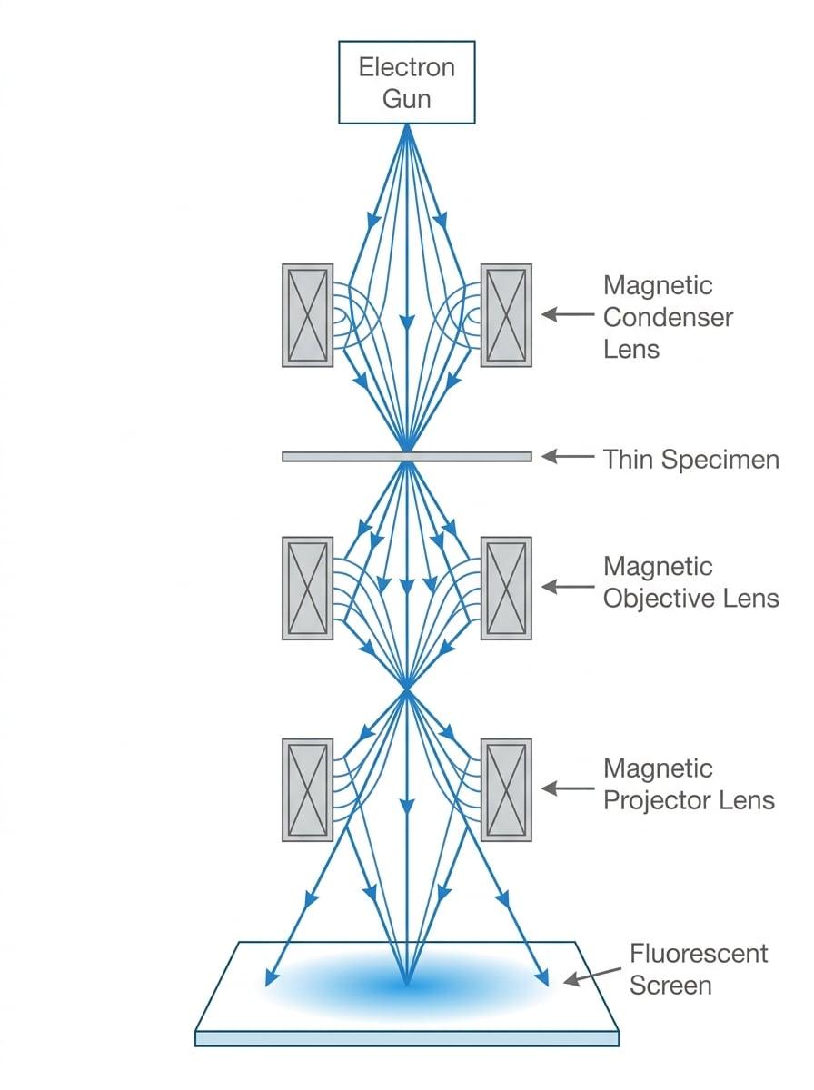
How a TEM works
- Electron Gun: A heated filament emits electrons, which are accelerated downwards by a high positive anode voltage.
- Condenser Lens: A magnetic lens deflects the diverging electrons into a wide, parallel beam that evenly illuminates the sample.
- The Specimen: The sample must be extremely thin (often less than 100 nm100 \text{ nm}100 nm). Electrons pass through it. Where the sample is denser, electrons scatter more, creating "shadows" in the beam.
- Objective Lens: This magnetic lens forms the first, highly magnified image of the sample.
- Projector Lens: This magnifies the image further and projects it onto a fluorescent screen or a digital detector.
Sample thickness matters
If the sample in a TEM is too thick, the electrons passing through will undergo multiple collisions. They will lose kinetic energy, which causes their momentum to drop and their wavelength to increase (λ=hp\lambda = \frac{h}{p}λ=ph). A larger wavelength results in a lower resolving power, creating a blurry image.
Limitations of the TEM
Even though the theoretical resolving power of a TEM is incredible, practical issues limit the actual resolution:
- Lens Aberrations: Magnetic lenses cannot focus electrons of slightly different speeds perfectly to the same point. Since electrons emitted from the hot filament have a tiny spread of initial kinetic energies, they arrive at the lens with slightly different speeds (chromatic aberration).
- Vacuum Requirement: Electrons are easily scattered by air molecules, so the entire interior of the TEM must be a hard vacuum. This means living specimens cannot be observed.
The Scanning Tunnelling Microscope (STM)
The Scanning Tunnelling Microscope (STM) uses a completely different physical principle. It does not use lenses to form an image. Instead, it relies on a strange quantum effect called quantum tunnelling.
In classical physics, if an electron does not have enough energy to overcome an energy barrier (like the physical gap between two metals), it cannot cross. However, because of its wave nature, an electron's wave function extends slightly past barriers. If the gap is small enough, there is a small but finite probability that the electron will simply "tunnel" through the gap and appear on the other side.
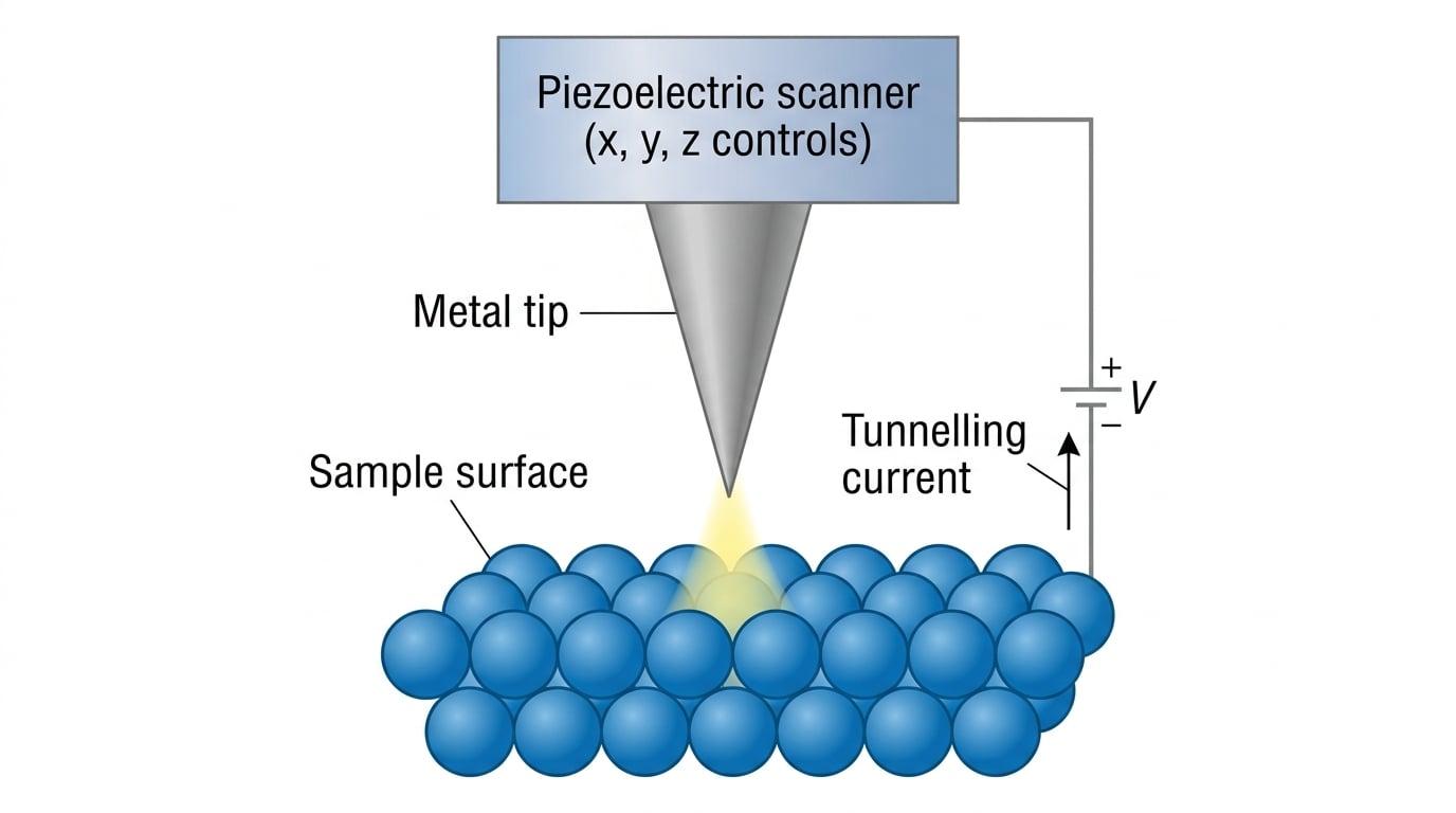
How an STM works
The STM maps the microscopic contours of a surface using an incredibly sharp, conducting probe.
- The Probe: The tip is manufactured to be as sharp as possible, ideally ending in a single atom.
- The Gap: The tip is brought extremely close to the surface being scanned (about 1 nm1 \text{ nm}1 nm away) without touching it. A small voltage is applied between the tip and the sample.
- Tunnelling Current: Electrons tunnel across the gap, creating a tiny electric current.
- Mapping: The probe is moved across the sample in a raster pattern.
The probability of tunnelling—and therefore the size of the tunnelling current—is highly sensitive to the width of the gap. Even a change in gap distance of an atom's width causes the current to change by a factor of 1000!
Piezoelectric Transducers and Constant Current Mode
To achieve the sub-nanometre precision required to move the probe, the STM uses piezoelectric transducers. These are special crystals that expand or contract by tiny, precise amounts when a voltage is applied across them.
The most common way to operate an STM is constant current mode:
- As the tip scans horizontally over a bump (an atom) on the surface, the gap gets smaller, and the tunnelling current begins to increase.
- A feedback circuit detects this and immediately applies a voltage to the vertical (zzz-axis) piezoelectric transducer.
- The transducer contracts, lifting the tip slightly until the current returns to its original, constant value.
- By recording the voltage applied to the zzz-transducer as the tip moves in the xxx and yyy directions, a computer builds a precise 3D topographical map of the atomic surface.
In the exam
When asked to explain the operation of these microscopes, keep your points precise and logical:
- For anode voltage calculations, always start by combining Ek=eVE_{\text{k}} = e VEk=eV and Ek=p22mE_{\text{k}} = \frac{p^2}{2 m}Ek=2mp2. examiners prefer you to show the derivation rather than memorising the final combined formula.
- For the TEM, state that the wavelength limits the resolving power. Be ready to explain why sample thickness reduces resolution (collisions →\to→ lower speed →\to→ lower momentum →\to→ longer wavelength).
- For the STM, clearly state that the probe does not touch the surface. Emphasise the role of the piezoelectric transducers in moving the tip and the feedback loop keeping the tunnelling current constant.
Check yourself
- Can you derive the equation linking accelerating voltage VVV and de Broglie wavelength λ\lambdaλ?
- Why are the 'lenses' in a TEM magnetic rather than glass?
- If a TEM specimen is too thick, what happens to the resolving power, and why?
- How does the size of the tunnelling gap in an STM affect the tunnelling current?