Revision notes for Edexcel GCSE Computer Science Von Neumann architecture and FDE cycle. Open the guide for explanations and worked examples. Written against the Edexcel GCSE Computer Science (1CP2) specification, so the content matches what's examinable rather than general Computer Science background.
Von Neumann architecture and FDE cycle
What you'll learn
- What the von Neumann stored program concept means.
- The roles of RAM, the CPU, registers, the clock, and the three main buses.
- How the fetch-decode-execute cycle works.
- How to describe the cycle using correct GCSE terminology.
The big idea: a computer runs instructions
A program is a sequence of instructions. An instruction is a single command that the processor can carry out, such as loading data, adding values, comparing values, or storing a result.
Computers store instructions and data in binary, which means using only 0s and 1s. The CPU does not directly “understand Python” or “understand a game” — it runs low-level binary instructions that have been loaded into memory.
The von Neumann stored program concept
Definition
Von Neumann stored program concept
The von Neumann stored program concept is the idea that program instructions and data are stored together in main memory, and the CPU fetches instructions from memory one at a time to run them.
Before von Neumann-style stored programs, some machines had to be physically rewired or reconfigured to perform a different task. With the stored program concept, changing the program means changing the instructions stored in memory.
This is the basis of modern general-purpose computers: the same hardware can run a web browser, a game, a word processor, or a Python program, because different instructions can be loaded into RAM.
Key Idea
Same memory, different meaning
In von Neumann architecture, a binary pattern in RAM could be an instruction or data. The CPU treats it according to where it is in the program and what the current instruction says to do.
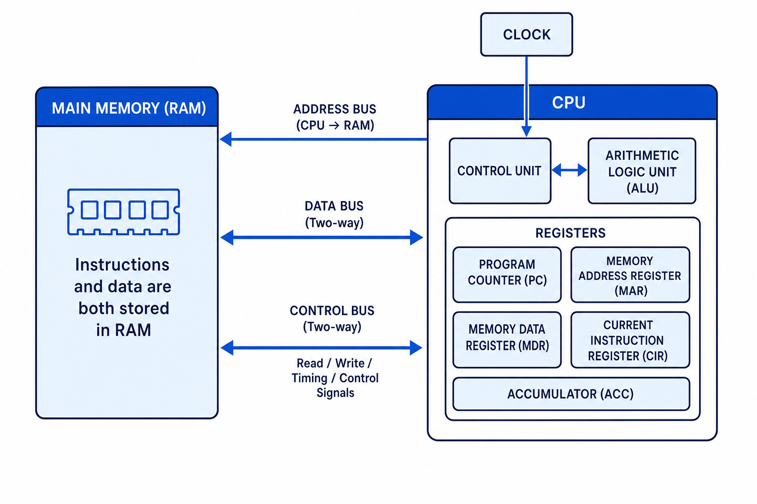
The diagram below shows the main parts of a simple von Neumann system: main memory, the CPU, registers, the clock, and the buses that connect them.
Main memory: RAM
Main memory is the memory directly accessed by the CPU while a program is running. In this topic, main memory means Random Access Memory (RAM).
RAM stores the programs and data currently in use. For example, when you open a game, the game’s instructions and the data it needs are loaded from secondary storage into RAM so the CPU can access them quickly.
RAM is volatile, meaning its contents are lost when the power is switched off.
Common Mistake
RAM is not long-term storage
The CPU fetches instructions from RAM during the fetch-decode-execute cycle. Programs may be saved long-term on secondary storage, but they must be loaded into RAM before the CPU can run them.
Memory addresses
A memory address is a unique location number in memory. You can think of RAM as a huge set of numbered boxes. The CPU uses an address to say which box it wants to read from or write to.
The CPU
Definition
CPU
The Central Processing Unit (CPU) is the processor: the part of the computer that fetches, decodes, and executes instructions.
The CPU contains several important parts.
Control Unit
The Control Unit (CU) coordinates the CPU. It controls the fetch-decode-execute cycle, sends control signals, and manages the movement of data between memory, registers, and the ALU.
During the decode stage, the control unit works out what the current instruction means.
Arithmetic Logic Unit
The Arithmetic Logic Unit (ALU) performs arithmetic and logical operations.
Arithmetic operations include addition and subtraction. Logical operations include comparisons such as checking whether one value is equal to another or whether one value is greater than another.
Registers
A register is a very small, very fast storage location inside the CPU. Registers temporarily hold data, addresses, or instructions while the CPU is working.
| Register | Role |
|---|---|
| Program Counter (PC) | Holds the address of the next instruction to fetch. |
| Memory Address Register (MAR) | Holds the memory address currently being accessed. |
| Memory Data Register (MDR) | Holds data or an instruction being transferred to or from memory. |
| Current Instruction Register (CIR) | Holds the instruction currently being decoded or executed. |
| Accumulator (ACC) | Holds intermediate results from calculations. |
Tip
Register names tell you their jobs
MAR contains an address. MDR contains the data being transferred. CIR contains the current instruction. PC points to the next instruction.
The clock
The clock is a timing signal that produces regular pulses. These pulses synchronise the activities of the CPU.
The clock does not store data and does not execute instructions by itself. Its job is to keep the CPU’s operations coordinated, so actions happen in the correct order.
A faster clock can allow more CPU cycles per second, but overall performance also depends on other factors, such as cache, number of cores, and how efficient the program is. For this topic, focus on the clock’s role in timing and synchronisation.
Buses
Definition
Bus
A bus is a set of wires or connections that transfers signals between components, such as between the CPU and RAM.
A von Neumann system uses three main buses.
| Bus | Main role | Usual direction |
|---|---|---|
| Address bus | Carries the memory address being accessed. | Usually CPU to memory. |
| Data bus | Carries data or instructions between CPU and memory. | Two-way. |
| Control bus | Carries control signals, such as read, write, and timing signals. | Often two-way. |
Address bus
The address bus carries the address of the memory location the CPU wants to access. If the CPU wants the contents of memory address 140, the address bus carries 140.
Data bus
The data bus carries the actual contents being transferred. This might be a data value, or it might be an instruction being fetched from RAM.
Control bus
The control bus carries signals that say what kind of operation is happening. For example, the control unit might send a read signal when it wants RAM to send back the contents of a memory address, or a write signal when it wants RAM to store a value.
Example
Choosing buses for a memory write
A CPU needs to store the value 23 in memory location 140.
- The CPU places 140 on the address bus, because RAM needs to know which memory location to use.
- The CPU places 23 on the data bus, because this is the value being transferred into RAM.
- The control unit sends a write signal on the control bus, so RAM knows to store the value rather than send a value back.
Common Mistake
Mixing up address and data
The address bus carries where to access. The data bus carries what is being transferred. Do not say the address bus carries the instruction itself.
The fetch-decode-execute cycle
Definition
Fetch-decode-execute cycle
The fetch-decode-execute cycle is the repeating process where the CPU fetches an instruction from memory, decodes what it means, and executes it.
This cycle happens again and again while a program is running. Each instruction goes through the cycle, although some instructions may need extra memory accesses during execution.
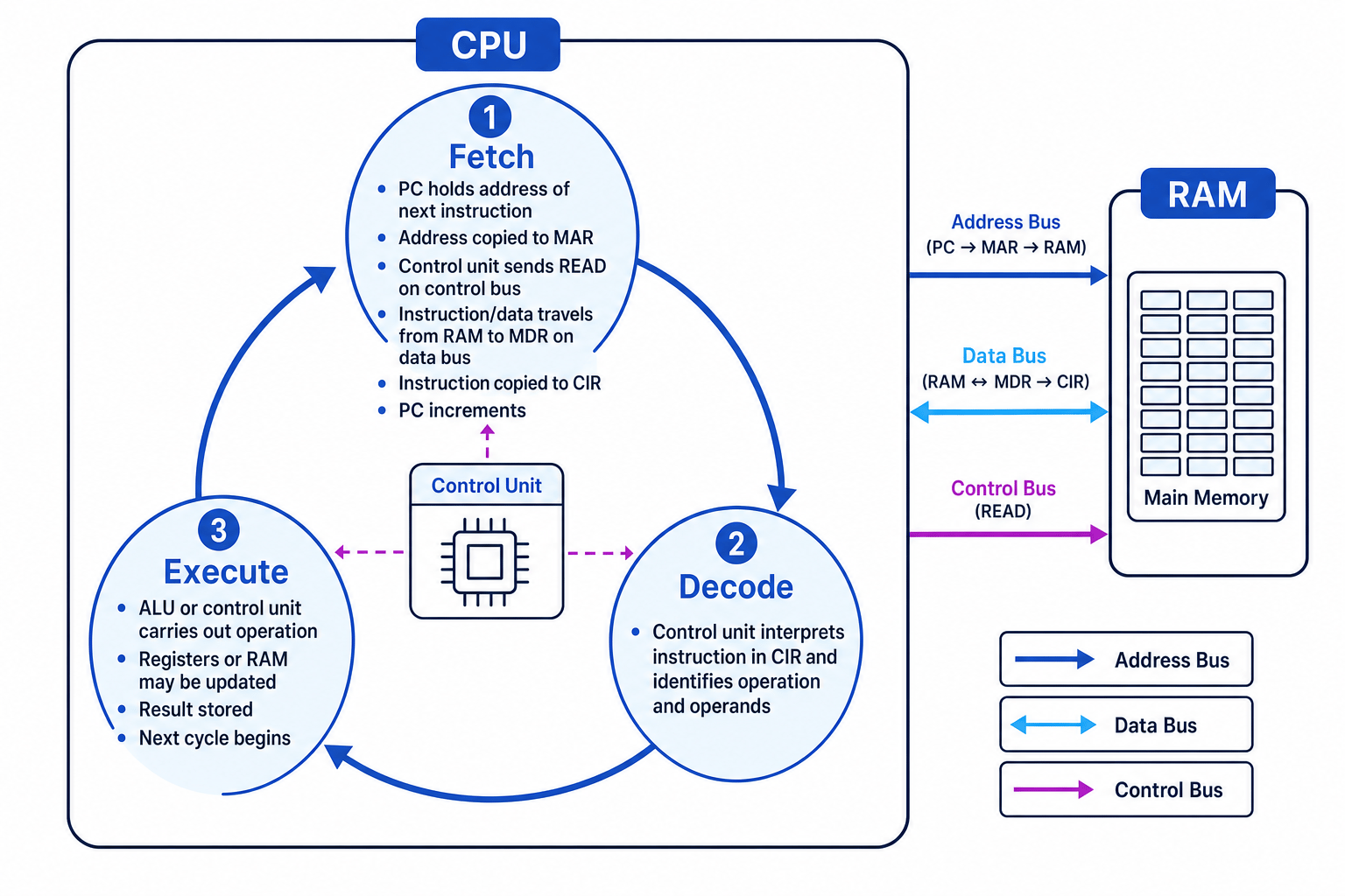
The diagram below shows how the CPU, RAM, registers, and buses are involved in the fetch-decode-execute cycle.
Stage 1: Fetch
During fetch, the CPU gets the next instruction from RAM.
A typical GCSE description is:
- The Program Counter (PC) holds the address of the next instruction.
- This address is copied into the Memory Address Register (MAR).
- The address is sent along the address bus to RAM.
- The control unit sends a read signal along the control bus.
- RAM sends the instruction back along the data bus into the Memory Data Register (MDR).
- The instruction is copied into the Current Instruction Register (CIR).
- The PC is incremented so it points to the next instruction.
Stage 2: Decode
During decode, the control unit interprets the instruction in the CIR.
It works out:
- what operation is needed, such as add, compare, load, or store
- which data or memory address is involved
- which CPU components need to be used next
For example, an instruction might mean “add the value stored at memory address 12 to the accumulator”. The control unit identifies both the operation and the memory address involved.
Stage 3: Execute
During execute, the CPU carries out the instruction.
This might involve:
- the ALU performing a calculation or comparison
- data being loaded from RAM into a register
- data being stored from a register into RAM
- the PC being changed if the instruction is a jump or branch
After execution, the CPU starts the next fetch.
Common Mistake
Branches can change the next instruction
Most instructions allow the PC to move on to the next address, but a jump or branch instruction can replace the PC with a different address. That is how loops and selection can happen at machine level.
Example
Tracing a simple instruction
Suppose the PC contains 40, and memory address 40 contains an instruction meaning “add the value at address 12 to the accumulator”. The accumulator currently holds 5, and memory address 12 holds 7.
- The CPU fetches the instruction at address 40: the PC value is copied to the MAR, 40 is sent on the address bus, a read signal is sent on the control bus, and the instruction travels from RAM to the MDR and then to the CIR. The PC is updated to 41.
- The control unit decodes the instruction in the CIR and identifies that it must add a value from memory address 12 to the accumulator.
- The CPU needs the operand, so 12 is placed in the MAR, the address bus carries 12 to RAM, and a read signal causes RAM to send the value 7 back on the data bus into the MDR.
- The ALU adds the value in the accumulator, 5, to the value from memory, 7. The result, 12, is stored back in the accumulator, and the next cycle begins using the instruction address now held in the PC.
Putting the roles together
The fetch-decode-execute cycle is not just “the CPU does three things”. It is a coordinated process involving memory, registers, buses, the control unit, the ALU, and the clock.
Key Idea
One cycle, many components
RAM stores the current instructions and data. The CPU controls and processes them. Registers hold temporary values. The buses move addresses, data, and control signals. The clock keeps the whole process synchronised.
Exam technique
In the exam
- If asked to describe the fetch stage, use the key register names: PC, MAR, MDR, and CIR.
- Keep the three buses separate: address bus carries where, data bus carries what, and control bus carries read/write/control signals.
- Link each CPU part to its role: the control unit coordinates and decodes, the ALU performs arithmetic/logic, and registers temporarily store values inside the CPU.
Self review
Check yourself
- What does the von Neumann stored program concept say about instructions and data?
- During fetch, what is copied from the PC to the MAR, and which bus carries it to RAM?
- Why does the data bus need to be two-way, while the address bus is usually from CPU to memory?
You've reached the end
Test yourself on this topic, or move on to the next guide.
How was this guide?