MOSFET (metal-oxide semiconducting field-effect transistor) (A-level only)
What you'll learn
- The basic structure and terminals of an N-channel enhancement mode MOSFET.
- How to interpret the characteristic voltages and currents (VDSV_{DS}VDS, VGSV_{GS}VGS, IDSSI_{DSS}IDSS, and VthV_{th}Vth).
- Why the MOSFET's near-infinite input resistance makes it a brilliant electronic switch.
- How to solve potential divider circuits designed to turn a MOSFET on and off.
Meet the MOSFET
A MOSFET (Metal-Oxide Semiconductor Field-Effect Transistor) is a semiconductor device that acts as an electrically controlled switch or amplifier. While you might have seen bipolar junction transistors (BJTs) before, which are controlled by current, a MOSFET is controlled purely by voltage.
For AQA A-Level Physics, you only need to know about one specific type: the N-channel, enhancement mode MOSFET.
To understand how it works, we first need to look at its internal structure.
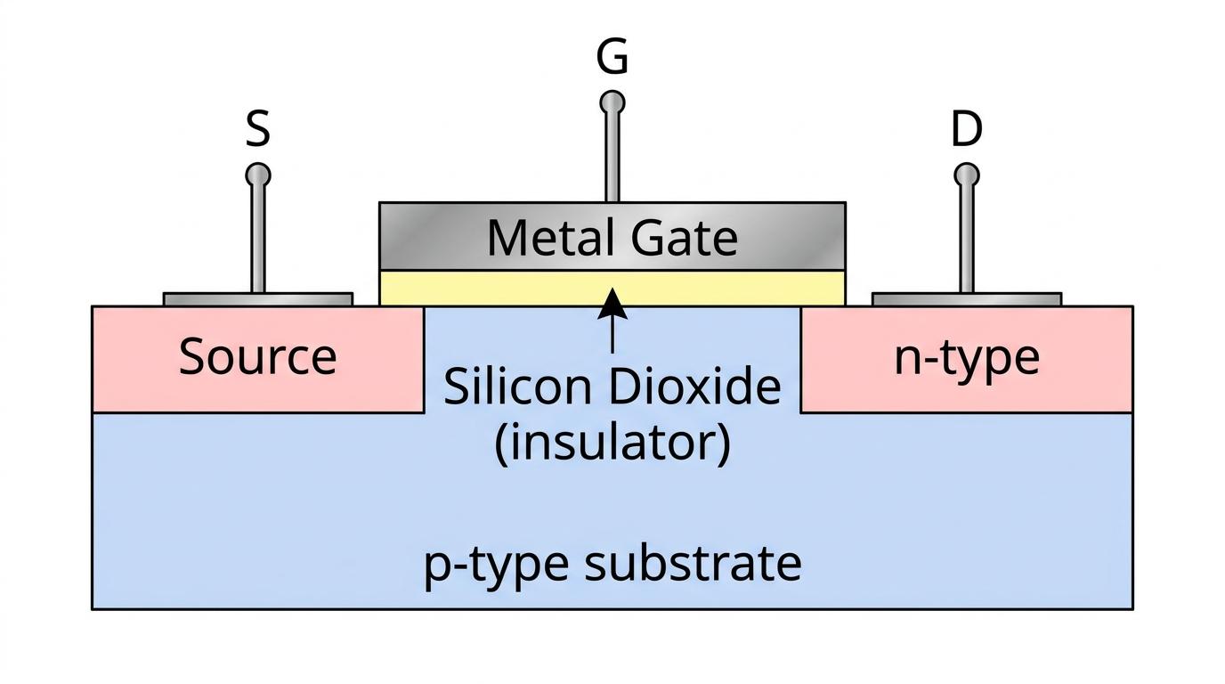
MOSFET Terminals
A MOSFET has three main connections (terminals):
- Gate (G): The control input.
- Source (S): Where the main charge carriers enter the device.
- Drain (D): Where the main charge carriers leave the device.
Notice the insulating oxide layer (usually silicon dioxide) sitting immediately directly below the Metal Gate. This is the most important structural feature of the MOSFET! Because the Gate is completely insulated from the rest of the semiconductor, no current can flow into the Gate terminal.
High Input Resistance
Because of the insulating oxide layer, the resistance between the Gate and the rest of the device is practically infinite (often hundreds of giga-ohms). We say the MOSFET has a very high input resistance. This means it draws effectively zero current from whatever sensor or circuit is trying to control it.
How the MOSFET Turns On (Enhancement Mode)
By default, an N-channel enhancement mode MOSFET is OFF. If you apply a voltage between the Drain and the Source (VDSV_{DS}VDS) but leave the Gate alone, no current will flow because the P-type substrate blocks the path between the two N-type regions.
To turn it on, we must apply a positive voltage to the Gate relative to the Source. This is called the Gate-Source Voltage, or VGSV_{GS}VGS.
When VGSV_{GS}VGS is positive, it creates an electric field that pushes positive "holes" away from the oxide layer and attracts negatively charged electrons up toward it. This gathers a thin, temporary bridge of electrons directly under the Gate. Because this bridge is made of negative charge carriers, it is called an N-channel.
Threshold Voltage
- VthV_{th}Vth (Threshold Voltage): The minimum Gate-Source voltage (VGSV_{GS}VGS) required to create the N-channel and allow current to start flowing from the Drain to the Source.
Since we are "enhancing" the conductivity of the device by applying this voltage, this is called enhancement mode.
- If VGS<VthV_{GS} < V_{th}VGS<Vth, the MOSFET is OFF (acts like an open switch).
- If VGS≥VthV_{GS} \ge V_{th}VGS≥Vth, the N-channel forms, and the MOSFET turns ON (acts like a closed switch).
Determining the MOSFET State
A student builds a circuit containing an N-channel enhancement mode MOSFET with a threshold voltage Vth=2.4 VV_{th} = 2.4\text{ V}Vth=2.4 V. They apply a gate-source voltage VGS=1.8 VV_{GS} = 1.8\text{ V}VGS=1.8 V and a drain-source voltage VDS=5.0 VV_{DS} = 5.0\text{ V}VDS=5.0 V.
Determine whether current flows between the Drain and the Source, and explain why.
- State the condition for the MOSFET to turn on: the applied gate-source voltage must be greater than or equal to the threshold voltage (VGS≥VthV_{GS} \ge V_{th}VGS≥Vth).
- Compare the given values: the applied VGSV_{GS}VGS is 1.8 V, but the required VthV_{th}Vth is 2.4 V.
- Conclude that since VGS<VthV_{GS} < V_{th}VGS<Vth, the N-channel is not formed.
- State your final answer: No current flows between the Drain and the Source because the MOSFET remains in its OFF state.
Characteristic Voltages and Currents
Once the N-channel is open, current can flow. The current flowing into the Drain is called the Drain Current, IDI_DID. The amount of current that flows depends on both VGSV_{GS}VGS (how "wide" you open the channel) and VDSV_{DS}VDS (how hard you push the electrons across it).
We can plot how IDI_DID changes as we increase VDSV_{DS}VDS. This gives us a family of output characteristic curves.
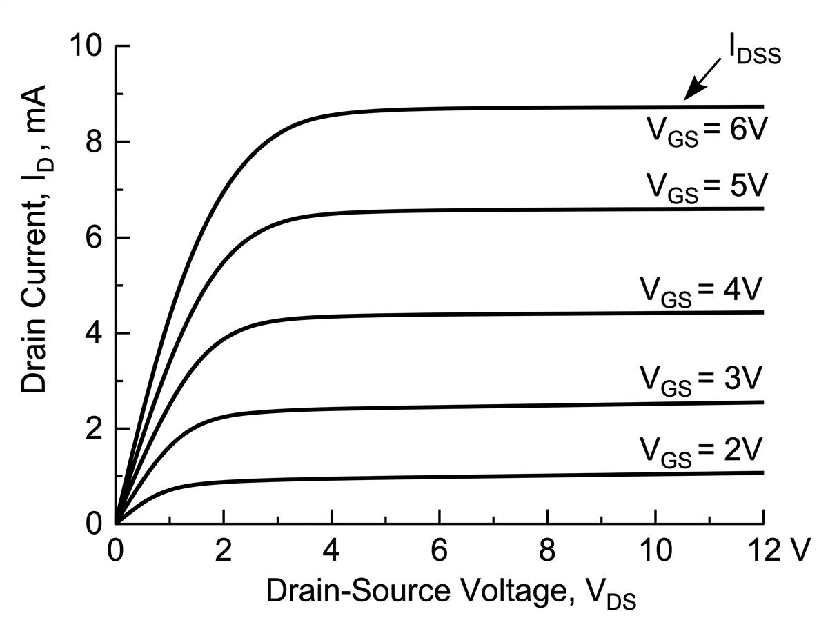
Look closely at the graph:
- The rising slope: At low values of VDSV_{DS}VDS, the current IDI_DID increases roughly proportionally to the voltage. Here, the N-channel is behaving a bit like a standard ohmic resistor.
- The plateau (Saturation): As VDSV_{DS}VDS increases further, the current stops rising and flattens out into a horizontal line. The MOSFET has reached its maximum current capacity for that specific Gate voltage.
Drain-Source Saturation Current
- IDSSI_{DSS}IDSS (Drain-Source Saturation Current): The maximum constant current that flows through the MOSFET when it is fully saturated (the flat part of the curve). A higher VGSV_{GS}VGS will result in a higher IDSSI_{DSS}IDSS.
Power Dissipation in Saturation
An N-channel enhancement mode MOSFET is operating in its saturation region. The gate-source voltage is held constant such that the saturation current is IDSS=2.5 AI_{DSS} = 2.5\text{ A}IDSS=2.5 A. The drain-source voltage is VDS=12 VV_{DS} = 12\text{ V}VDS=12 V. Calculate the power dissipated by the MOSFET.
- Recall the electrical power equation:
- Identify that the current flowing through the device is IDSSI_{DSS}IDSS and the voltage across it is VDSV_{DS}VDS.
- Substitute the values into the equation:
- Calculate the final answer:
Confusing the Voltages
Do not mix up VGSV_{GS}VGS and VDSV_{DS}VDS!
- VGSV_{GS}VGS is the tiny control voltage on the input side that decides if the switch is open or closed.
- VDSV_{DS}VDS is the usually much larger power voltage on the output side that actually pushes the main current through the load (like a motor or lamp).
Using the MOSFET as a Switch
The most common A-Level application for a MOSFET is using it as an electronic switch controlled by a sensor (like a thermistor or an LDR).
Because the Gate has virtually infinite input resistance, it draws zero current. This is perfect for potential divider circuits, because we can connect the Gate to the middle of the divider without it "stealing" any current and messing up the voltage calculation!
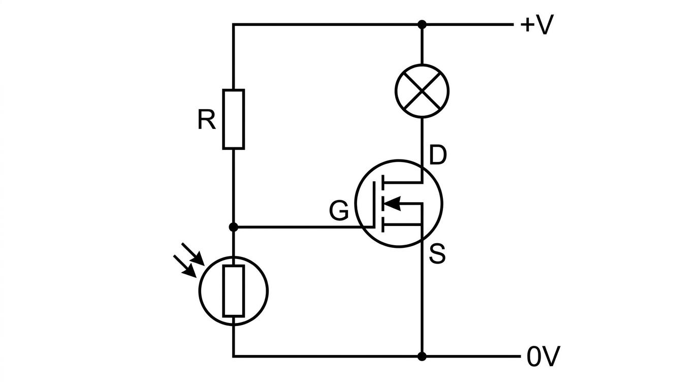
In the circuit above, the LDR and the fixed resistor form a potential divider across the supply voltage. The Gate is connected to the midpoint. When the light level changes, the resistance of the LDR changes, which changes the voltage at the midpoint. If that voltage (which is VGSV_{GS}VGS) rises above VthV_{th}Vth, the MOSFET switches on, allowing a large current to flow through the Drain and light the lamp.
Designing a Switching Circuit
A switching circuit is designed to turn on a heater when the temperature drops. The circuit uses a 12 V DC supply, a fixed resistor R1R_1R1, and a thermistor RthR_{th}Rth as a potential divider. The fixed resistor R1R_1R1 is at the top, and the thermistor RthR_{th}Rth is at the bottom, connected to 0 V. The midpoint connects to the Gate of a MOSFET with Vth=4.0 VV_{th} = 4.0\text{ V}Vth=4.0 V. When the temperature drops to the target level, the thermistor's resistance is 5.0 kΩ5.0\text{ k}\Omega5.0 kΩ. Calculate the required value of R1R_1R1 to ensure the MOSFET turns on at exactly this temperature.
- Identify that the voltage across the thermistor is the Gate-Source voltage (VGSV_{GS}VGS), because the thermistor is connected between the Gate and the 0 V line (Source).
- For the MOSFET to just turn on, we need VGSV_{GS}VGS to equal the threshold voltage:
- Use the potential divider equation, where VoutV_{out}Vout is VGSV_{GS}VGS, R2R_2R2 is the thermistor, and VinV_{in}Vin is the 12 V supply:
- Substitute the known values into the equation:
- Divide both sides by 12:
- Rearrange to solve for R1R_1R1:
- Calculate the final resistance:
In the exam
- State the mode clearly: If asked to describe the device, always explicitly state that the AQA specification uses the N-channel, enhancement mode MOSFET.
- Mention the infinite input resistance: If a question asks for the advantages of a MOSFET over other switches (like a BJT), write down "it has a very high input resistance" and follow up with "so it draws negligible current from the input circuit". This is almost always a 2-mark pair.
- Assume zero Gate current: When calculating voltages in a potential divider connected to a MOSFET Gate, assume the divider formula works perfectly. You do not need to account for current branching off into the Gate.
Check yourself
- What does the term "enhancement mode" tell you about the default state of the MOSFET when VGS=0V_{GS} = 0VGS=0?
- Which physical feature of the MOSFET is responsible for its extremely high input resistance?
- If you increase the Gate-Source voltage (VGSV_{GS}VGS), what happens to the saturation current (IDSSI_{DSS}IDSS) on the characteristic graph?